


Thank you for your solutions. That M2 connector appears to be like good, I didnt know about this type to attach boards 2 boards. Soldering these things by hand seems labouring to me, and as you level out that it’s somewhat a pain… Impatient as I am I continued to work out some concepts. And I feel the best commerce off between prices, labour and area is to use plain 2.0mm male and feminine connectors. The baseboard get’s a SMD male header. This safes space and isn’t that labouring to solder as the 2.0mm pitch is relative giant. That connector additionally has SDA, SCL, 485 A, 485 B and an analog pin routed. One of the boards will likely be I2C slave and the opposite is the master. Their software will be equivalent and they can tell which is who by way of soldering a single resistor on the service board to make a restistor divider. The mating controller gets a THT feminine.
Like der ule points out, those connectors I wanted are referred to as bottom-entry or prime or backside entry. Unfortunately JLCPCB don’t have any in inventory (for as far as I can find). They do exist in their stock listing. So I don’t know if they will ever come in their inventory. As such I selected for THT. And i might redesign the contoller with out that much work ought to I swap to a backside-entry connector. Those 3 solder pads on the underside are the handle pins for the EEPROM. The master controller should be ready to use the eeprom of an adjacent slave though this won’t be wanted… I do know the way to smd solder, that is not a difficulty but I merely do not want to solder at al. It is just way more cheaper to let a jlcpcb do that for me. I already get me sufficient work to solder the management panel itself. Anyways, thanks all for your contributions. I’ll keep these m2 connectors in mind.
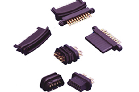
The PCB pins can legitimately be referred to as the muse of each PCB design. Similar to the best way PCBs do, pins function just like the interconnect system in addition to numerous plug-in purposes. The circuit board design does certainly have a big amount of performance thanks to hooks. Circuit board pins could be pushed in to circuit, swaged, and, for many circumstances, soldered it to Circuit board as a way to attach them to it. A obligatory conductive channel for the electrical circuit is provided by PCB pins. Because the mechanical interface, it offers an assembly module energy. What are the Common PCB connector types? How Can PCB Connector Be Tested? So as to attach two components and maybe a circuit board electrically, PCB header pins is often employed. Although there are numerous completely different sorts of PCB header pins, they are usually male connectors organized inside a row and spaced apart by a set distance and range.
Such components which can be difficult to mount on typical connectors or circuit boards are incessantly mounted using the PCB pin socket. The PCB pin socket is often used on the Circuit board to select such options having single contact factors. The ranges as well as dimensions of PCB pin sockets make it easier for shoppers to pick a number of of their choices primarily based on their needs. During current years, press-match pins have developed, making it less complicated for engineers and designers to make use of the press-fit and solderless connectors. Here’s more information about High-Speed PCB connector buyer guide visit the internet site. The PCB pins remain easy to make the most of and produce the technique of production less expensive as well as being extra accessible in contrast to the conventional strategies. The engineer will discover it a lot simpler to debug a circuit in this situation. The components put in on the Circuit board are mechanically supported by PCB alignment in addition to PCB guide pins. However, PCB solder pins is among the many most often utilized PCB pins when such connectors are hooked up to the circuit board high.
Their typical makes use of are within the creation of circuit boards and prototypes. Jumper pins on PCBs are frequently utilized to offer a path of conduction over a bypass element of an electrical circuit that’s open or closed. They are essential as a result of the bypass connection should be made for the digital parts utilized in PCB board by the designer. The PCB terminal pins have been made to meet the increasing needs of the electronics sector. The PCB’s terminal pins provide separate, excessive-present connections. The designer can create multiple set up schemes to serve the designs because of the varied kinds and PCB header connector patterns of the PCB pins. Engineers now find it a lot less complicated to function on prototypes or completed PCB designs due to PCB pin advances and enhancements. Many additional intricate patterns that would have seemed not possible to perform utilizing standard methods have now been made viable thanks to these breakthroughs. How Does a PCB Connector Work?